dCS Ring DAC - A Technical Explanation

Part 6 – Filter Design in ADCs and DACs

How do the digital audio filters discussed in Part 5 work, and how should they be designed? This may sound counterintuitive, but the filtering required in both ADCs and DACs is actually very similar.

In an ADC, the audio is coming into the converter at a higher rate than we want to output – typically by a power of 2. To deal with this, the converter must remove content above the Nyquist frequency, which allows it to drop samples (allowing it to lower the sample rate from 88.2k to 44.1k for example) without content from above the Nyquist frequency aliasing down below it. This is handled in Digital Signal Processing by way of low-pass filtering.

In an oversampling DAC, audio is coming in at a lower rate than we want to feed to the converter. There are several approaches for how to tackle this issue, but by far the most effective is to insert samples with an amplitude of zero between the actual audio samples to increase the sample rate, then low-pass filter the signal to remove the Nyquist images this process creates. Once again, DSP is used to implement low-pass filtering.

How is this digital low-pass filtering carried out? In simplified terms, the digital audio signal is run through a series of ‘coefficients’ – multipliers which change the amplitude of the audio sample by an amount, defined by a number between 0 (no output) and 1 (the original full amplitude of the sample). Each of these coefficients is what is referred to as a ‘tap’. A higher number of taps means the signal is run through a larger amount of coefficients in the filter. The output of the filter at any one point is the sum of all of these coefficients multiplied by the respective samples.

Audio websites and magazines often feature ‘impulse response’ plots of filters in audio products. These typically show the output from a filter when it is given samples, all with an amplitude of zero, then a single full-scale (all 1s) sample, then all zero samples again. The effect of this is to show the coefficients in a filter, which define how the filter works. Typically, this filter is a derivative of what is known as the ‘sinc’ function. The sinc function is defined as sin(x)/x and looks a little like the below graph.

image

There are several useful properties of the sinc function – it acts as an ideal low pass filter (the set of coefficients used in a digital filter, as previously described, are taken from this function, hence the Y axis being shown as ≤1, which will be shown below); it is mirrored in time in both directions (before and after the impulse, the single full-scale sample shown in the middle of the above sinc graph) and it offers the same delay at all frequencies (not all filters do this). An analogue filter will delay some frequencies more than others, creating phase issues. Filters which offer the same delay at all frequencies are referred to as phase linear.

Given these factors, the sinc function can be manipulated to provide the desired frequency response. The three main factors that can be adjusted with digital filters are:

  • The -6dB point – the frequency at which the filter reaches 6dB of attenuation.
  • The filter length – the number of coefficients used in the filter, with one coefficient often being referred to as a ‘tap’.
  • The windowing technique – this is linked to both of the above factors (this is a simplified explanation).

Cutoff Frequency (-6dB Point)

To explore the factor of the cutoff frequency of a filter, take the below graph, which shows the most commonly used digital filter. This is a ‘half-band’ or ‘Nyquist’ filter, with coefficients based off of the sinc function. This filter is designed in such a way that the -6dB point is at the Nyquist frequency of our target. For a low-pass filter in, for example, an ADC, the Nyquist frequency is set at 22.05kHz. For a tap length of 128, this generates the below impulse response.

image

The crucial aspect of this filter is that every other coefficient (the data points on the graph marked by an X) is 0 – which makes it twice as computationally effective as a non-Nyquist filter (as using a coefficient of 0 always results in an output of 0). The drawback to this type of filter is that by definition it only reaches 6dB attenuation at the Nyquist frequency. Thus, aliasing artifacts from the ADC which will be mirrored down to below Nyquist frequency will not be correctly attenuated. We would therefore ideally want the -6dB point to be below the Nyquist frequency, to remove said aliases and to maintain good attenuation at the Nyquist frequency.

image

Windowing Technique

There are some drawbacks to using the sinc function as the basis for a digital filter – firstly, the filter would be infinitely long (due to the sinc function being a mathematical function with no defined length), which is problematic in the real world. It also requires data from the future, as the filter coefficients include data from before the current sample being played. So how should these issues be addressed?

A good start would be to define the filter as not infinitely long. Doing so would allow the incoming audio signal to be buffered by a certain number of samples. This means the filter can then effectively have some data from the ‘future’ by delaying the entire audio signal by that amount of samples.

However, defining the filter with a finite length leads to some mathematical problems – the sinc function starts to get very small when moving further away from the central impulse, but not so small that the function becomes irrelevant. Sinc is infinitely long, but it is unwise to simply select a finite section of the sinc function to use as the basis for a filter, chopping off the ‘start’ and ‘end’ of the function to create a finite length. Doing so actually causes the resultant filter to not work very well. The below graph shows an example of a digital low-pass filter designed to work for CD rate audio, with a tap-length of 64 taps, where the ends of the sinc function have simply been chopped off to provide the coefficients used in the filter.

image

As can be seen from this graph, this filter does not provide a good response. The stop-band rejection above 22.05kHz is poor, and there is a significant ripple in the passband (below 22.05kHz). This problem is best addressed through a technique called ‘windowing’. This involves taking the coefficients for the filter we want to use, such as a finite section of the sinc function, and then multiplying them by another set of coefficients to reduce the negative effects seen above.

There are many approaches to windowing (different sets of functions / coefficients) used, but for this example, a raised cosine window will be used.

image
This diagram shows an example of a Raised Cosine window.

Applying this window to the above 64-tap filter results in the below frequency response:

image

As can be seen, this provides drastically better results. The stopband has far better rejection and the rippling seen in the passband is no longer present. What this means is that when designing a filter for use in audio, the windowing function needs to be selected carefully for correct filter performance.

Filter Length

The third factor to consider with filter design is the length of the filter itself. As previously discussed, we need to filter the output of a DAC to prevent imaging. This filter needs to be a finite length – longer than nothing but not infinitely long. If this is not done and no filtering is carried out to the DAC’s output, and the samples are played back as they come in, the result is not ideal:

image
This graph shows the frequency response of a Non-Oversampling (NOS) DAC with no filter on the output.

As discussed in the previous article, a filter for 44.1k digital audio should not affect signals below 22.05kHz, but should heavily attenuate them above this. With no filter in place, not only is there very little attenuation above 22.05kHz (thus leading to lots of false high frequency components), we are also affecting the signal we are interested in: the frequency response at 20kHz is -3dB.

So, how long should the finite length filter on the DAC output be? To illustrate this factor, the same previously mentioned Nyquist filter with a raised cosine window will be used. Firstly, a 32 tap filter:

image

image

As can be seen from the above graphs, the frequency response is still far too droopy to be appropriate for use – at 20kHz, the response is still down about 2.8dB. Attenuation for images above 33kHz (or for images in the region of 0-11kHz) are 50dB down. The transition band width is in the region of 20kHz.

Next, the same Nyquist filter with a raised cosine window will be used, but this time with a length of 256 taps:

image

image

This response is visibly much better. The pass-band response is very flat up to 20kHz, and the transition band is approximately 4kHz wide. Images above 22.05kHz are supressed nicely. Looking at the impulse response however, it can be noted that much more data from before the current sample is playing is required. As such, a larger number of samples from ‘the future’ are required for this filter and will subsequently be having an impact on the current sample, and more samples from ‘the present’ will have an impact later on.

Lastly, using the same example upped to 1024 taps:

image

image

As can be seen here, lengthening the filter has a few effects. Firstly, the transition band has become much narrower, so there is less out of band energy. There are, however, some negative effects – because there are more coefficients performing more multiplies, the stopband noise rejection is actually starting to degrade. Noise is beginning to accumulate in the stop-band (which can be partly compensated for with the windowing). There are also now a large amount of samples from the ‘future’ being used (in this example of 2014 taps at 44.1k, around 11mS worth) and an equal amount will be affected in the ‘past’. The effects of these factors are debatable, but where these samples come from has to be considered. With that in mind, a good real-world example…

dCS 904 – 44.1k, Filter 1

image
This graph shows the frequency response of the dCS 904 running at 44.1kS/s using Filter 1.

This graph shows the filter frequency response from a very capable ADC, used in many recordings – a dCS 904. The first thing to note about this example is that it doesn’t use a Nyquist filter like the examples above. The attenuation by the Nyquist frequency is 20dB. This is important as an ADC, by definition, deals with signals that are not bandlimited. The final filter is around 100 taps long, meaning that effectively there is little to be gained from using a much longer filter on replay (inside the DAC). Considering what this response means, the following chart is helpful:

image

This graph helps to illustrate the area of uncertainty caused by this filter. In the intersecting area, it isn’t possible to differentiate between real signal and an alias. As such, use of excessively long filters here leads to heavy use of DSP to preproduce what is effectively the transition band of the ADC – signal which is undesirable, and unknown.

What this stands to show is that with digital filter design, the signal chain as a whole needs to be considered, as opposed to just the DAC in isolation. DAC filters which are likely to work well with realistic ADC filters are ideal – in reality the use of a filter which is either not present, too short or too long in a DAC can have detrimental effects. Filter length of course must be balanced with the other factors described above, which is where good engineering comes into play – understanding how to employ the necessary trade-offs to create a set of filters which work well regardless of what content is thrown at it. This is the reason a dCS DAC has so many filters to choose from – the DAC doesn’t (and can’t) know the filters which were used to create the signal, so several options allow the user to achieve the best musical experience irrespective of source material.

dCS’s experience with both ADCs and DACs leaves us in a very strong position to be able to create DAC filters which consistently perform to the highest standards, both in testing and with real-world musical signals.

9 Likes

Hi folks,

Following our series on D/A conversion, we have a new set of posts to share. These posts will focus on another important aspect of the D/A conversion process, which is clocking. Whilst a DAC’s circuitry is responsible for making sure the right voltage is generated on conversion (ideally without correlated errors), clocking is responsible for ensuring the conversion happens at the right time. This series aims to explore why this is important in digital audio, along with good practices related to clocking.

We’ll start with discussing the basics of clocking and what happens when clock systems fail to produce an accurate signal. We’ll also examine the effect this causes, jitter, and the consequences this can have on digital playback, before going on to look at clock synchronisation in audio systems with multiple components, and the role of clocking in relation to asynchronous audio, such as music streamed over the internet or played via USB. Alongside this, we’ll provide an insight into the design of both dCS clock systems and dCS Master Clocks, and explain the steps we take to ensure our clocks deliver an accurate and consistent signal.

Our aim is to provide some helpful information on the role and importance of clocking in digital audio, and answer some common questions related to this topic, as well as providing a deeper look at our approach to developing clock systems and Master Clocks (something we’ve been doing for over three decades). We hope you’ll find it useful.

2 Likes

Part 1 - The Basics of Clocking

Clocking is an integral part of digital audio, and almost all audio products have a clock inside. As discussed in our previous series on digital to analogue conversion, digital audio recordings are made up of a series of samples. An audio product such as a DAC has to know when to do something with the samples it receives at its input, whatever this task might be – and this is where clocks come in.

In the context of digital electronics, the term clocking refers to a signal that keeps all of the circuits within a system in sync and operating at the same time. In order to generate a precise and reliable signal, the clock system must have a source: something that defines how long a period of time is. This source usually comes in the form of an oscillator – an electrical circuit that provides a regular rising and falling of voltage.

At dCS, we use quartz crystal oscillators as the basis for our clock systems. Quartz is a piezoelectric material, meaning that when a voltage is applied to it, it physically deforms and flexes back and forth. The crystal can be designed to resonate mechanically at a particular frequency (for example, every 44,100th of a second) and with a correctly designed electrical circuit, this resonance can be converted into an oscillating voltage.

The frequency of the crystal’s resonance lets a system know how long a specific increment of time (such as 1/44,100th of a second) is. Through measuring these increments of time, a system can accurately space audio samples apart. This avoids any unwanted movement of the samples in time, which, if it occurred during the digital to analogue conversion process, could cause distortion of the audio signal heard during playback.

The design of clocks in digital audio (both internal clock systems and external master clocks) is a topic worthy of serious consideration when purchasing any high-end audio system. Arguably, clocking can have as much of an impact on sound quality as DAC circuitry, and it’s vital to consider the design and implementation of the clocking system as a whole, rather than selecting simply selecting components that have an impressive specification on paper.

As the clock defines the timing of a DAC’s operations, it is responsible for ensuring the samples are converted at the correct time, which is crucial to ensuring the audio we hear during playback sounds as it should.

Jitter

If a clock system fails to produce a signal correctly during the D/A conversion process, or the signal is unable to correctly reach a DAC, then we experience something called jitter, which is highly undesirable in audio.

Jitter is described as any irregularity in the timing of the clock used by a DAC, and it is produced in a variety of ways. It can be the result of bad analogue design, electromagnetic interference, poor quality digital audio cable or a number of other causes, which we’ll discuss in future posts.

The actual audible effect of jitter depends upon its nature, but it can have a notable impact on sound. If jitter is periodic, sidebands will appear either side of the signal frequency. This sounds like a harsh distortion, as artificial components are being added to the audio. If the jitter is noisy in nature, this results in a ‘smearing’ of signal energy. This, in turn, increases the noise floor of a system, which has the effect of masking fine detail in the music.

The above graphs show an example of what can happen with poor clocking. In both examples, a sine wave has been reconstructed by a DAC using 25 samples. Each of these samples has exactly the same amplitude in both graphs; the only factor which has changed is the timing of when several of the samples are converted. The result is a visible degradation of the signal. Were this signal to be played back through a transducer, the signal in the lower graph would sound noticeably worse than the top due to the jitter.

While the example above is rather exaggerated, it illustrates that the right sample at the wrong time is the wrong sample. This goes to show just how vital accurate clocking is to a digital audio playback system.

The human ear and brain are extremely sensitive to irregularities in the timings of sound. If a DAC experiences jitter, and fails to convert signals into analogue voltages at the correct time, then the sense of space in a performance can be heavily skewed or even lost. It’s for this reason that dCS engineers take great care to minimise jitter in all aspects of our design.

If jitter is introduced at the recording stage, it will remain in the signal forever. There are steps that can be taken to prevent further degradation of the signal (such as re-clocking or even buffering the signal into RAM and out again) but it isn’t possible to correct or remove jitter that arises during the recording process.

At the playback stage, jitter should be minimised wherever possible to avoid the signal we hear being compromised or altered. Provided a recording is of decent quality, having a DAC reproduce audio samples at exactly the right moment will help to ensure that listeners experience an accurate representation of the original sonic event. A signal coming into a DAC from an external source, such as a CD transport, can actually have very irregularly spaced samples on arrival (to a point, which we’ll cover in future posts), but provided the DAC itself converts those samples at regular intervals, the sound quality will remain unaffected.

Our next two posts will cover the main kinds of jitter: intrinsic and interface.

9 Likes

Once again thanks James. What fascinating series . How many other manufacturers would even bother?

2 Likes

Many other DAC manufacturers don’t have much to write about - they use a standard DAC chip, choose/implement some filters and analog stages and that’s it. Pretty short stories I’d say :wink:

3 Likes

Part 2 - Jitter (intrinsic)

There are two main kinds of jitter: intrinsic and interface. Intrinsic jitter refers to jitter which is produced inside of a product like a DAC, through effects like phase noise on the oscillator. Interface jitter refers to jitter which is picked up by the interface(s) used to transfer the audio and clock signals. This could come either as interference picked up by the cable itself, or through the cable essentially acting as a filter for certain frequencies, impacting the integrity of the square wave (the output of the clock circuitry) passing through it.

There are several varieties of quartz crystal oscillators, but Voltage Controlled Crystal Oscillators (VCXOs) and Oven Controlled Crystal Oscillators (OCXOs) are two of the most common in audio.

Voltage Controlled Oscillators, or VCOs, are also used in audio products, but these operate on a purely electronic basis, and do not use an electromechanical material such as quartz to generate signals.

Quartz oscillators tend to have better phase noise performance than VCOs, meaning the oscillator itself may be less prone to jitter. What this means in terms of overall clock design is that in a DAC with a quartz oscillator, the Phase Locked Loop, or PLL (the circuit which matches the frequency of the DAC’s clock to the clock of the incoming audio signal) can be biased towards rejecting interface jitter by means of a narrower PLL bandwidth.

This is possible as the quartz oscillator itself is less prone to phase noise and subsequently jitter. As such, if jitter should happen to be present on the interface, for example a jittery AES signal, this jitter will not be passed on to the DAC, as it will have come and gone before the PLL reacts to it. The DAC instead relies more on the oscillator for timing accuracy between individual samples which, in the case of a dCS product and its quartz crystal-based clock, is a very high level of accuracy.

The alternative to this would be to use a VCO as the oscillator. However, given the potentially poorer phase noise performance of a VCO compared to a quartz oscillator, the PLL within the product may need to be biased towards rejecting intrinsic jitter, as the oscillator itself would likely be more prone to phase noise, which can be achieved through using a wider bandwidth PLL. This means any interference or cable filtering effects will have a more direct impact on the sound which, in some use cases, may be undesirable.

If this is the case, you might be wondering why any product would use a VCO as a clock source. One benefit of using a VCO over a quartz oscillator is the possibility for the clock to have a greater ‘pull range’, meaning it can lock to a wider range of signals (for example, signals running consistently too fast or too slowly).

In our experience, in the context of a high-end digital audio playback system, the quality of a DAC’s clocking should not be permanently compromised to allow for a sub-optimal source to be connected and work properly. At dCS, we opt for using a quartz-based oscillator with a high level of accuracy and stability, allowing for a pull range of +/- 300 parts per million (PPM), as per AES specification.

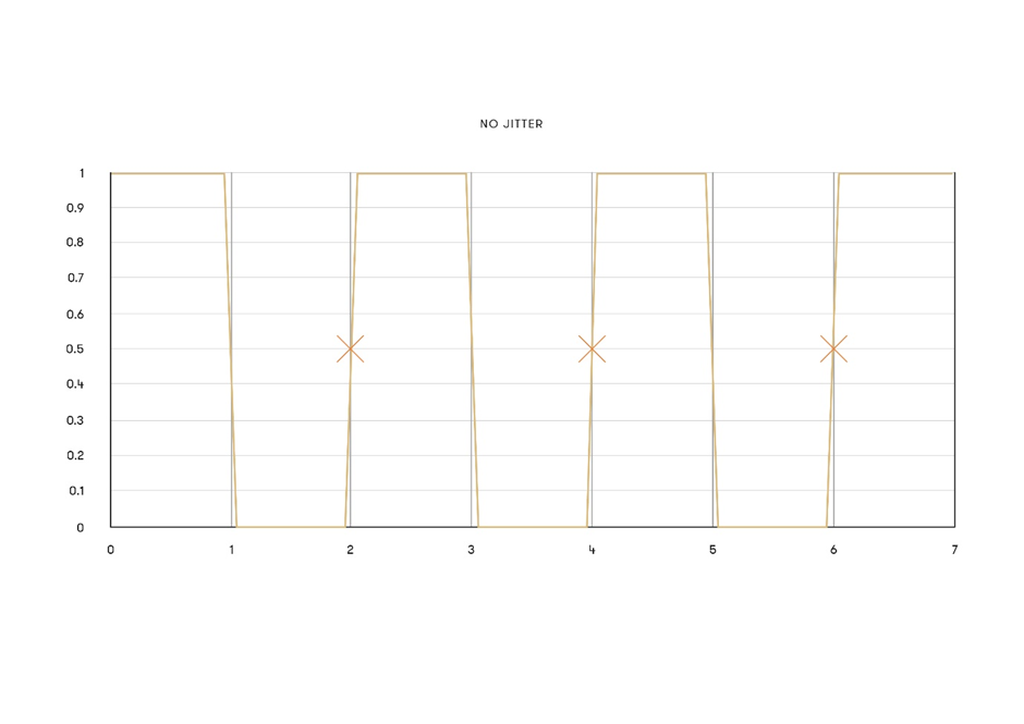
These graphs show an exaggerated example of the effect of jitter on the square wave output by a clock circuit. As previously discussed, jitter has both impacted the transition times of the wave and the peak voltages the wave can reach. This has the effect of changing the point at which the system would perceive, for arguments sake, a 0 changing to a 1. Clock systems watch the ‘rising edge’ of the clock signal where the voltage increases, so the point on the rising edge where the amplitude goes above 0.5 has been marked on the graphs. The timing of this is regular in the first graph – the transition points on the rising edges fall on 2, 4 and 6 on the X axis respectively. When jitter is introduced, the transition points are shifted forwards or backwards depending on the nature of the jitter. It is not regular, it is random.

There are several factors that can cause phase noise (and, consequentially, jitter) on an oscillator, and these should all be taken into account when designing a clock system.

Physical Vibrations

As the basis of a quartz clock is its piezoelectric property (the physical movement of the crystal when a voltage is applied), any external physical vibrations can cause inaccuracy in the clock. The extraneous movement does not need to be vigorous to cause inaccuracy. It could be as subtle as, for example, the vibrations of a CD mechanism inside the product. Any measures which can be taken to isolate the clock circuitry from the external physical vibrations should be taken, as this creates a higher level of clock performance.

Power Supply

The ability of a quartz crystal (or any piezoelectric material) to maintain a consistent oscillation frequency relies on having a stable, interference-free DC signal of the correct specification. In the case of both VCXOs and OCXOs, this means clean DC for the power supply. In the case of a VCXO, even more crucially, the control voltage needs to be stable (in this type of oscillator, the control voltage is used to make fine adjustments to the crystal’s frequency). If there is any variation in the power rails fed to the crystal, the frequency it resonates at will change. In products with a quartz-based clock, designers should always endeavour to have as clean a power supply fed to the crystal(s) as possible, at the correct voltage and frequency for the specification of the region the product is being used in.

Crosstalk

Electronic circuits can generate electromagnetic leakage. This is often seen when running high-rate signals such as digital audio signals through the copper tracks found on PCBs (printed circuit boards). The copper tracks essentially act as antennas, with the digital audio signals being radiated from the board. This interference can have an impact on associated clock circuits if they are in close proximity, negatively impacting the performance of the clock.

The correct way to eliminate this issue is to design the product’s PCBs in such a way that minimises crosstalk. Secondary to this is to ensure that any sensitive parts are separated from those which may cause interference. An even more effective method is to completely remove many potential sources of EM interference from the product, where possible, such as with the use of a Master Clock (a standalone clock with its own dedicated circuitry and power supplies).

Clock Frequency

The ideal way to design the clock inside an audio product is to have two oscillators: one running at direct multiple of 44.1kHz, and the other running at a direct multiple of 48kHz. The reason for this is that almost any sample rates used in digital audio are multiples of these ‘base rates’ (including DSD, which runs at very high multiples of 44.1kHz). If the clock does not use direct multiples of the sample rate it is to be clocking, the maths becomes more complex and the electronics that need to be used to generate the correct frequency are more prone to jitter.

Trying to clock a 44.1kHz signal with a 10MHz clock, for example, would require somehow synthesising 44.1kHz from 10Mhz, which mathematically is not clean. As such, this type of clock will need to use methods such as asynchronous rate conversion to multiply the rate down correctly. These methods invariably result in a ‘dirtier’ frequency spectrum of the clock signal, meaning that the system will be more prone to jitter.

dCS products use two oscillators, running at 2^9 of the base audio rates (44.1kHz and 48kHz), so 22.5792MHz and 24.576MHz. The easy division down to any required rate results in a cleaner clock spectrum and, as a result, less jitter.

Clock Temperature

While clock temperature is not a source of phase noise, it can affect the performance of an oscillator. The resonant frequency of a quartz crystal is inversely proportional to its size and, by extension, its temperature. As the temperature of the quartz increases, it physically expands. As the temperature decreases, it contracts. This causes changes in the resonant frequency of the quartz, as the physical size is now different. Temperature variations in digital systems should therefore be avoided, or the effects mitigated wherever possible.

There have been several methods for counteracting temperature variations inside a crystal oscillator. One approach is to use an industry-standard OCXO. An OCXO aims to remove the temperature variation of the crystal by using a Curie heating element to keep it at a stable temperature. The Curie device is a resistive heater whose resistance increases sharply when it reaches a certain temperature, effectively cutting back the heating power. The temperature will overshoot and then stabilise around the required temperature. When the temperature of the product is not stable (such as when it is powered on from cold), due to thermal delays, there will be some fluctuation in the temperature and, consequently, the frequency as the system ‘hunts’ around the target temperature. Once the crystal’s temperature has stabilised, however, the clock will output a stable frequency.

Another approach is to use a microcontroller-enhanced VCXO, as we’ve done in a number of dCS products. This approach does not use any heating elements to account for temperature variation. Instead, we utilise the large amounts of processing power available thanks to the FPGA-based design of our products to make constant adjustments to the control voltage fed to the VCXO to compensate for temperature changes.

In the case of a dCS Master Clock, such as the Rossini Clock or Vivaldi Clock, these adjustments are based on intensive measurements taken during production. During the production process, we place the clock (and the circuit board the clock is fixed to) into an Environmental Chamber. This chamber measures the clock frequency against the current controlled environmental temperature and records it onto the FPGA inside the product. The temperature is then changed, the clock measured, and the performance again logged. This process is repeated over 18 hours. This enables us to plot exactly how the VCXO in the Master Clock behaves at any given temperature, which the product has a record of.

This data is actioned in the product by adjusting the control voltage which is fed to the VCXO. A higher or lower voltage will create a higher or lower resonant frequency. This, combined with the product’s knowledge of its performance against temperature, ensures the clock’s output frequency is always stable. At any given normal operating temperature, the clock’s output frequency will be consistent.

This is a constant process inside the Rossini and Vivaldi Clocks, with the clock temperature regularly measured, and the control voltage adjusted if the clock temperature has varied. The result is that a new Vivaldi Clock, for example, can achieve an accuracy of above +/- 1 PPM when shipped. Once the clock has stabilised in its environment, the accuracy typically increases to +/- 0.1 PPM.

In the next post, we’ll look at the other main kind of jitter: interface jitter.

Part 3 - Jitter (Interface)

10 Likes

Very interesting, thanks James.
Merry Christmas!

That’s a good description of why clocks aren’t calibrated at home, too. Golly. What a process!

Thanks so much for these posts, dCS people :+1:

Excellent series. One aspect of clocking that I hope you will address has to do with the provision for an externally attached “master clock” for the Vivaldi Clock. What type of clock should this be if used? And what would be it’s overall value with other components, which rely on clocking, within a consumer audio system? I’m thinking here of network switches of maybe CD playback or streaming devices.

Part 3 – Jitter (Interface)

If a product is locking to the clock signal of an external source, such as a CD transport connected to a DAC, interference picked up by digital audio cables between the products can smear the transition times of the clock data within the signal – essentially, changing the point in time where a 0 changes to a 1, or vice versa.

Balanced lines help reduce interference induced in the cables. This is why the AES/EBU format uses 110Ω twisted-pair, shielded cable. This effectively shields the conductors in the cable from most electromagnetic interference (EMI) and flushes any that it picks up to ground, eliminating it from the signal. Any EMI that gets through to the conductors gets phase-cancelled, because each conductor is exactly 180 degrees out of phase with the other. (Since the pairs are run together, any noise will be induced in both conductors in phase with each other and, thus, cancelled.)

It’s important to ensure that a cable has the bandwidth needed for digital signals. The square waves carrying the signal have a very fast rise time between the low and high states (the 0s and 1s). A fast rise time translates to a very high frequency – up in the megahertz range. For this reason, it’s advisable to use good quality 110Ω cable for AES transmission and 75Ω cable for S/PDIF transmission that is specifically designed to carry digital audio data.

When a digital signal is passed through a cable, the cable will, to a degree, act as a filter. A poorly designed cable, which is unfit for use with the interface it is designed for (such as AES3, for example) could potentially filter out high frequencies from the signal before it reaches the DAC from the source device.

This causes an interaction between any two consecutive data bits within the signal, called intersymbol interference. Depending on the relationship between the first and second of any two bits, the transition between the two can be temporally smeared. The ideal clean vertical line of the square wave becomes more sloped, meaning the exact moment a 0 changes to a 1 or vice versa can be blurred. In short, jitter can be introduced purely from the interactions within the data itself.

If the timing data in the audio signal is being used to lock the DAC’s clock to the source’s clock, this intersymbol interference will have a negative impact on sound quality, as it can introduce jitter to the DAC’s clock. However, if the audio system is making use of a Master Clock, and the timing information embedded in, for example, the AES3 signal is no longer being used, the effects of intersymbol interference are negated. While the same filtering effect in the cable and interactions within the data occur, the intersymbol interference does not cause jitter. This is because the Word Clock signal being sent from a Master Clock is regular and does not change like an AES signal does.

It is worth noting that as the PLL used in a dCS product is slow acting, and the clock recovery circuits used are very capable, the effects of intersymbol interference are minimised in cases where the DAC needs to lock to the clock information embedded in the audio signal (such as instances where a Master Clock is not available).

The next post will discuss clock synchronisation, such as how to utilise a Phase Locked Loop to synchronise two different clock domains, like those in a DAC and connected Transport.

Part 4 - Clock Synchronisation

6 Likes

Part 4 – Clock Synchronisation

There is a problem posed when multiple digital audio devices, each with their own internal clocks, need to work together. Take the example of feeding a CD transport into a DAC. The DAC has a buffer – a section of temporary memory which stores the audio samples it receives from the CD transport. The transport’s clock dictates when a sample is sent out to the DAC, and the DAC’s clock dictates when the sample is used and converted to an analogue voltage.

In an ideal world, the clocks in the DAC and transport would be running at the exact same rate with no time variations. In reality, however, there will be variations in the clocks on average (potentially caused by the intrinsic jitter factors discussed earlier). This poses a problem somewhat different to jitter.

If the clocks are running at different rates, on average, over a long period of time, and are left to their own devices with no method of synchronising the two, there will come a point where either the buffer in the DAC has used all of the available samples from the transport, because the transport is sending the samples too slowly / the DAC is using them too quickly, or the buffer overflows because the transport is sending samples too quickly / the DAC is using them too slowly. This will result in the audio dropping out temporarily, as the DAC must drop everything and relock to the audio signal to get audio samples flowing properly again.

There are two main ways to address this issue. Firstly, there are pieces of timing information embedded within the digital audio signal that the transport gives out in S/PDIF or AES format. The DAC can look at this timing information and adjust the speed of its own clock to match. This means the clocks of the source device and DAC will now be running at the same rate, so dropouts will no longer occur.

The second method that can be employed is to lock both the source and DAC to a Master Clock. A Master Clock is a unit which sits external to all other units in a system and provides a clock signal, referred to as Word Clock, to the rest of the system. The internal clocks of all other units within the system can then be locked to this signal, meaning that on average, they are running at the same rate as the Master Clock. This means that at no point should the DAC suffer from dropouts or re-locks due to the buffer under or overflowing, as on average, the samples are being sent from the source device at the same rate as they are being consumed by the DAC.

The common factor between these two methods is that they both require a method of synchronising an incoming signal with the product’s internal clock, by way of a PLL. There a number of DACS in the high-end market which do not have the ability to match their clock domain to that of an incoming source, as the oscillator(s) run at a fixed frequency. This means that the unit will drop or repeat samples every now and again (definitely not desirable behaviour) and will have variable latency, so cannot be used for video because of the resulting lipsync drifts.

As an aside, it is worth noting that the use of a Master Clock in a dCS system does not replace the internal clock inside of the DAC. It simply acts as a stable reference for the DAC to lock itself to, and allows for DAC and source to be properly synchronised without issues such as intersymbol interference causing jitter within the audio data. The DAC’s internal clock still dictates when samples are converted, it simply adjusts its frequency over time to match that of the Master Clock. This means the DAC still benefits from having a high-quality clock close to the DAC circuitry. The clock directly controlling the audio is still part of a tightly controlled environment, while also being in sync with the rest of the system.

Phase Locked Loops (PLL)

A Phase Locked Loop, or PLL, is a circuit that works to match the frequency of an incoming signal with that of an outgoing signal. They are often used to synchronise a DAC’s internal clock to that of an incoming signal, such as SPDIF from a CD transport. A ‘phase detector’ in the PLL attempts to match the phase of the incoming SPDIF signal with that of the DAC’s internal clock. Its aim is to get the phase error as low as possible, ensuring that over time, the two clocks run at on average the same rate, and the DAC’s buffer never under or overflows.

The most common place to see a PLL in an audio product is within an ‘off-the-shelf’ SPDIF receiver chip. This chip will be utilised on the SPDIF input of a product, typically combining an SPDIF to I2S block together with a PLL. Using a third-party solution such as this can give rise to some issues. With such a chip, it can be very difficult to separate out the functions of signal conversion and clock domain matching. This becomes problematic when attempting to use a Word Clock signal as the clock master for the DAC. What’s more, if the performance of the chip isn’t up to scratch, then it is impossible to change it. AES clock extraction is a good example. This is actually quite difficult to do well; because of the structure of illegal codes within the signal, it is easy to induce jitter from the channel block marker that occurs every 192 samples (the structure of SPDIF/AES is beyond the scope of this post but in essence, the signal deliberately breaks the ‘rules’ by having periods of 3 0s or 1s in a row for various reasons, including to lock the PLL to).

At dCS, we’ve taken a different approach. dCS DACs still use a PLL, but it is a hybrid design, developed entirely in-house. Part of the PLL is digital, by way of DSP inside the product’s FPGA, and part of it is analogue. This lends an enormous amount of flexibility, and a much higher level of performance. Additionally, it is completely independent from the input source. We are also able to carry out functions like dramatically altering the bandwidth of the PLL. This allows the DAC to lock very quickly to a source, thanks to a wide bandwidth on the PLL. The bandwidth can then be tightened over time to reduce jitter.

This approach ensures that, within a dCS product, the clock and data paths remain independent. There is a part of the product’s FPGA which works solely to extract the clock embedded in, for example, the incoming AES signal (again, this is done using a bespoke design, rather than an off-the-shelf chip); another part which works to retrieve the audio, another for routing it, then processing it, and so on.

This gives us a tremendous amount of flexibility in terms of how we handle, for example, Dual AES: we can run the signal, have a separate Master Clock input, have the DAC act as the Master Clock for the whole audio system, tolerate different lengths of cables in Dual AES, and deal with phase offset between clock and audio, and all of this can be done without adding latency to the audio, meaning it can still properly integrate with video. We are also able to hide commands embedded in the non-audio bits of AES, which allows us to have, say, the Vivaldi DAC (a non-network equipped product) controlled by the dCS Mosaic Control app.

This diagram shows a simplified example of how a digital source (a Rossini Transport), a DAC (the Bartók Headphone DAC) and a master clock (the Rossini Clock) work together. The overall performance of the system is reliant on each of these stages performing correctly – each oscillator, PLL and output stage needs to operate at a high level to achieve optimum performance.

Clock Dither

The setting for Dither can be found on the dCS Rossini and Vivaldi Clocks. Dither is commonly found in digital audio, where it is used to expose dynamic resolution below that of the least significant bit. In the aforementioned Clocks however, the dither is applied to the time domain instead of the amplitude domain.

PLLs exhibit what is known as a ‘dead band’ in their phase detectors. When the input and output frequencies are close to being synchronised, they lose sensitivity. The PLL then drifts until the difference in frequency is large enough to cause the phase detector to once again become active and drive the PLL back towards being synchronised.

This is where the dither comes in: Perhaps counter-intuitively, if very small, random variations in the timing of the clock signal edge are applied when the phase error is very low, it gives the PLL something to latch on to and correct (as it pushes the phase error slightly back into the area where the phase detector can correct well). The dither is then filtered out in the PLL before it outputs the final clock signal. In practical listening this is a good trade-off and actually improves system performance. In essence, the dither setting on the Rossini Clock keeps the Bartók DAC’s clock very accurate even when the PLL is working in a less sensitive, low phase error area.

Part 5 – Asynchronous Sources – USB & Network Audio​

10 Likes

Great stuff. This post is missing the link to the subsequent post at the end
Thanks
Rudi

The subsequent post is an explanation on what is dCS Apex…so only few days to read it :laughing:

Part 5 – Asynchronous Sources – USB & Network Audio

Audio sent over an asynchronous format (such as streaming to a smartphone via Spotify, playing content from a NAS via Roon, or playing music from a computer via USB) is, to an extent, the exception to the rules stated in the previous posts, in so much as jitter is not a factor for the audio data, at least until it reaches the endpoint and is converted back to the relevant format (such as PCM or DSD).

With network audio, the interface which is used to send audio data over a network is called TCP (Transfer Communication Protocol). The data which is to be transmitted from one place to another –
in this case a piece of music – is split up into multiple ‘packets’. These packets contain not only the data itself (the ‘payload’), but tags on where it has come from, where it is going, how many packets it is part of and how these packets should be reassembled to get the original data back unchanged.

Take, for example, a track from Qobuz being streamed to a dCS Bartók DAC. If a packet of data is lost or compromised, according to the TCP interface, the Bartók can simply request that packet again. When all the correct packets have been received properly by the Bartók, they are unpacked back to the correct data format (PCM, for example) and buffered before being fed to the DAC. This stage, the unpacking and buffering, effectively removes any timing link between the TCP packets and the resultant audio signal. (Read that sentence again, as it’s very important.)

Once the data has been buffered in the Bartók, the factors discussed above become relevant again. The data is now being directly dictated by the Bartók’s clock and as such, jitter becomes a factor. The accuracy of the Bartók’s clock then controls when the DAC converts the samples back to analogue voltages, so has a direct impact on audio quality. Until it reaches that point, however, jitter is simply not a factor from an audio perspective.

Asynchronous USB audio works in a similar way. There is no timing link whatsoever between the source, such as a computer, and the endpoint such as a Bartók. It does not matter if, while the USB data is being transferred, the bits are not perfectly spaced as a clean square wave. Provided the bits are received by the Bartók correctly (a 1 isn’t misread as a 0, for example) the timing is largely irrelevant. This is because, as with network audio, the data is buffered before being fed to the DAC. It is not until this point that timing becomes a factor, as at this point, it has been converted back from USB format to digital audio (eg PCM or DSD).

9 Likes

Indeed. Thanks for all this James. Superb information.

It means no need for any clocking system before the data are processed by the Upsampler, am I right ?

1 Like

Sounds so to me.

Correct. At least in terms of how clocking is discussed here. A digital device such as a network switch still has a clock but for very different purposes that are nothing to do with audio - the idea of externally ‘clocking’ something that is spitting out asynchronous data like a network switch is a bit of a contradiction.

4 Likes

Does it also means that my expensive Audioquest rj45 Vodka cable isn’t more useful that any cat 6 cable ? I am already sweating in waiting for your answer :laughing:

But I take the opportunity that you don’t sleep yet to tell you that it is a real privilege to sometimes have a chat with the designers of great gear I use every day to listen to music.
I share what Greg wrote in another thread, saying that he trusts the dCS engineers, me too, impatient to hear the new Apex :+1:

From a few of the more objective folks I have spoken to I believe the ethernet cable and switch are not in the critical signal path and won’t impact sound. They make fine audio jewelry. I am not an anti-cable guy I have a full high end loom of interconnects.

2 Likes